
Based on the basic principles of laser damage, researchers have found a breaking through point to solve the problem of laser damage to optical components. But it is very difficult to effectively suppress the source of laser damage in the manufacturing process. Given the variety and complexity of the manufacturing process of optical components, it is necessary to establish the link between the defect formation and the manufacturing process. Therefore, it is necessary to carry out specific research of the damage characteristics according to the manufacturing process of different types of optical components, and even to develop special detection and analysis methods for the defects of different component manufacturing processes. These personalized components and processes have become a continuous driving force of laser damage research. For example, the nodule defect in the multilayer dielectric film is the main cause of damage in the 1 μm laser band. It comes from the sputtering caused by the phase change when evaporating HfO2 materials. The Phase change and sputtering were inhibited by reactive evaporation of hafnium metal. The density of nodule defects is reduced by an order of magnitude, which meets the flux requirements of current ICF laser drivers. However, the laser damage to multilayer dielectric films in the triple frequency band (355 nm) originates from the nanoscale precursors at the interface of materials with high and low refractive index. Researchers have not yet formed a complete understanding of the characteristics and formation mechanism of the nanoscale precursors, and there is also a lack of completely effective method to control them. This problem will still be a research topic in the future.
Laser-induced damage on optical component
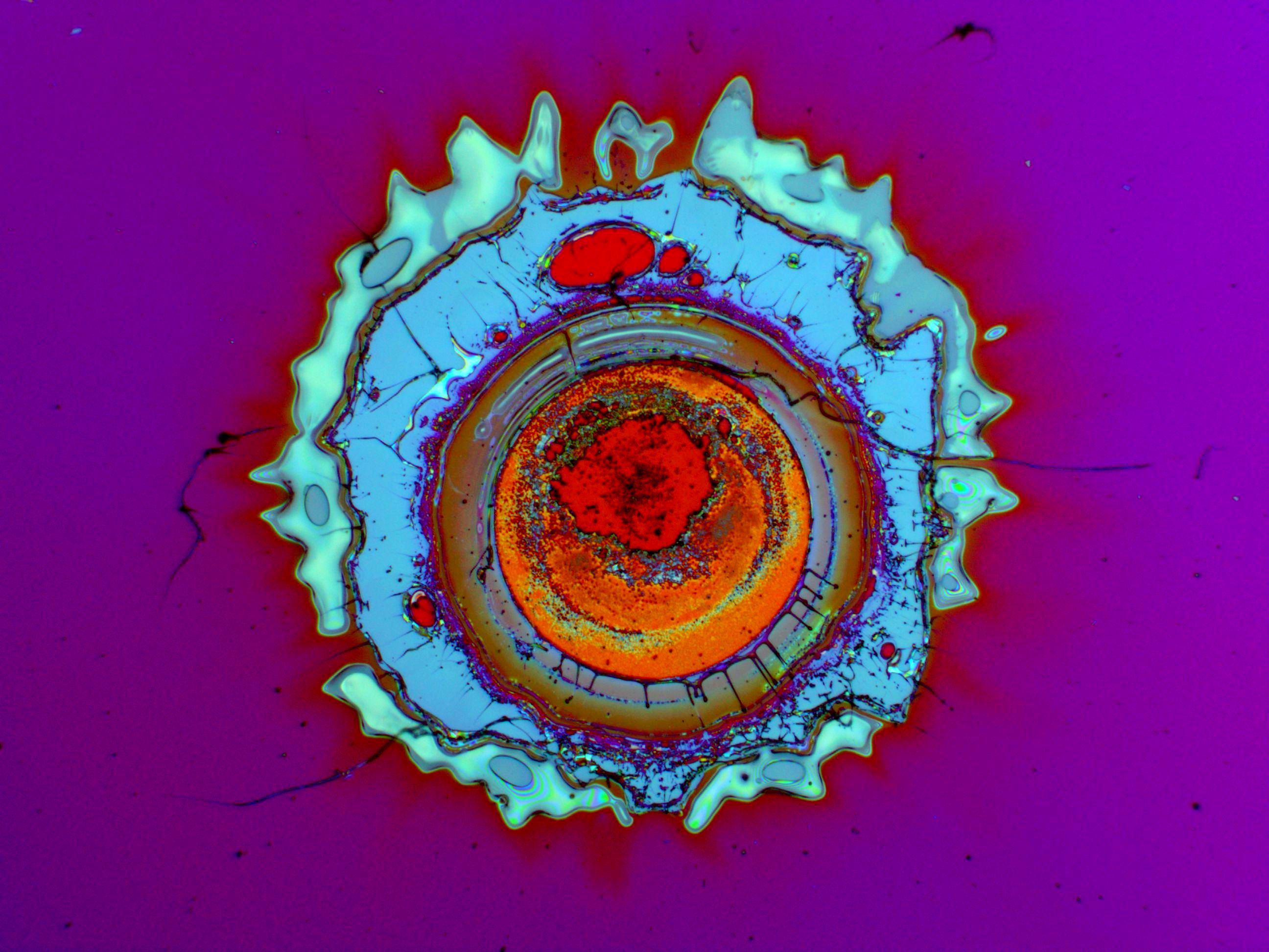
In order to control defects, the defect must first be found. The defect detection technology has become to be indispensable in the strong laser optical component industry. In a conventional sense, the defects of optical materials or optical components generally refer to inclusions, surface pits and scratches, etc. For laser damage research, the meaning of defects here is broader, including not only structural defects observable by optical imaging methods, but also other absorption defects that can lead to local enhancement of laser absorption. Due to the randomness and diversity of defects, high requirements are put forward for detection technology. The relationship between defects and laser damage must be established, and the source of defects must be traced to the process technology, so as to guide the optimization of manufacturing process of the optical element. Since it is difficult to establish online, in-situ, and real-time observation methods for laser-induced damage, it is tough to trace the source of these defects. It is often speculated through the analysis of the damage morphology and verified by defect implantation technology. This is effective for the study of defects with geometric shapes and microscopic scales, but it is difficult for nanoscale defects that cannot be resolved by conventional optical means.
Post time: Jan-15-2023